ELECTROCHEMICAL PREPARATION OF MULTISEGMENT NANOWIRES
I. Enculescu, E. Matei, M. Sima, M. Enculescu, R. Neumann
Meet. Abstr. - Electrochem. Soc. / MA2008-02 / E9 - One-Dimensional Nanoscale Electronic and Photonic Devices 2
Abstract 2145, ISSN: 1091-8213 (print) 2151-2043 (online)
Metal-semiconductor-metal multisegment nanowires were prepared by electrochemical deposition in nanoporous ion track polycarbonate membranes (the so called template method). The approach offers some very important degrees of freedom, i.e. the possibility to choose the desired density of nanopores by selecting the appropriate heavy ion irradiation fluence and the desired size and shape of the nanopores by using the appropriate etching conditions for the ion tracks. Thus one can employ templates with the desired characteristics: high pore density for measurements of optical, structural or morphological characteristics of the nanowires and low pore density membranes for electron transport characterization.
The present report deals with the influence of the preparation conditions on the properties of multisegment nanowires. The chosen semiconductor segment was of CdTe. Thus the influence of parameters such as deposition potential or temperature on morphological or structural properties were investigated. Moreover, differences between wires deposited at constant potential and in a pulsed regime were emphasized.
Transport properties were also investigated, special attention being paid to metal semiconductor contacts properties at nanoscale.
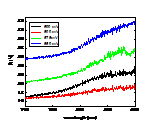
One important parameter for the deposition of a compound semiconductor is the deposition potential. In figure 1 the electrochemical polarization curve for the deposition of CdTe in a nanoporous membrane is presented.
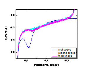
Figure 1. Polarization curves for CdTe in a nanoporous membrane (pore diameter 90 nm). Sweep rate 5 mV/s.
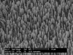
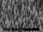
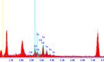
One can notice in figure 1 the plateau in the potential range -0.5V to -0.6V. This plateau represents the stoichiometric region. The scanning electron microscopy imaging and the EDX measurements proved that highly uniform, stoichiometric arrays of CdTe nanowires are obtained by electrochemical deposition (figure 2). Optical spectroscopy measurements were performed on the arrays of nanowires, from the reflection spectra the band gap of the compound semiconductor and the influence of the overvoltage in its value being calculated.
 |
 |
(a) |
(b) |
 |
 |
(c) |
(d) |
Figure 2. (a) and (b) SEM images of CdTe wires deposited at -500 and -550 mV respectively, (c) EDX spectra for CdTe nanowires deposited at -550 mV shows a near stoichiometric composition, (d) reflexion spectra of CdTe nanowire arrays.
For more electronegative potentials, wires with a high Cd content are obtained and is interesting to note that for a deposition potential of - 0.67 V vs. SCE the cobalt content reaches approximately 98 % due to the much higher content of cadmium ions in the deposition solution. This can be easily used in order to obtain multisegment metal semiconductor metal wires. Thus, it is not necessary to change the deposition solution in order to obtain more complex nanowires. This is extremely important in terms of reproducibility of the experiments.
The measurements performed on low density nanowire arrays showed that the deposition potential is also extremely important for fine-tuning the transport properties of the multisegment nanowires in both shape of the current voltage characteristics (i.e. one can tailor the type of metal semiconductor contact) or in terms of current versus temperature characteristics (a variation from semimetallic to semiconducting behavior being observed).
Thus the electrochemical deposition in template membranes can be employed not only to prepare simple semiconducting nanowires but also to obtain multisegment wires. Such more complex nanostructures have a wide range of potential application for example as ultraminiaturized photodetectors.
CENTRUL NATIONAL DE MANAGEMENT PROGRAME CNMP
Programul 4 Parteneriate in domeniile prioritare